The counter can be clocked
internally or externally through T0 pin (PD4, Arduino 4).
When clocked internally, the clock is passed through a
configurable prescaler. This is configured using the CS02:0
(Clock Select) bits on the TCCR0B (Timer/Counter Control
Register).
TCCR0B
(Timer/Counter Control Reg. B)
7
FOC0A
Force Output
Compare A
6
FOC0B
Force Output
Compare B
5
--
4
--
3
WGM02
Waveform
Generation Mode
2
CS02
Clock Select
1
CS01
0
CS00
CS02:0
Clock Selection
000
Timer/Counter stopped
001
Internal Clock clkI/O
010
Internal Clock clkI/O
divided by 8
011
Internal Clock clkI/O
divided by 64
100
Internal Clock clkI/O
divided by 256
101
Internal Clock clkI/O
divided by 1024
110
External clock on falling
edge of T0 pin (PD4, Arduino 4)
111
External clock on rising
edge of T0 pin
This counter has four
modes of operation configurable through WGM02:0 bits on
the TCCR0x registers. In the normal
mode, the counter always counts up and restarts from
0x00 when it reaches 0xFF.
TCCR0A
(Timer/Counter Control Reg. A)
7
COM0A1
Compare
Match Output A Mode
6
COM0A0
5
COM0B1
Compare
Match Output B Mode
4
COM0B0
3
--
2
--
1
WGM01
Waveform
Generation Mode
0
WGM00
WGM2:0
Operation Mode
TOP
Update of OCRx at
TOV0 set on
000
Normal
0xFF
Immediate
0xFF
010
CTC
OCRA
Immediate
0xFF
When the counter overflows, TOV0
(Timer/Counter Overflow Flag) is set.
TIFR0
(Timer/Counter Interrupt Flag Register)
7
--
6
--
5
--
4
--
3
--
2
OCF0B
Timer/Counter 0
Output Compare B Match Flag
1
OCF0A
Timer/Counter 0
Output Compare A Match Flag
0
TOV0
Timer/Counter 0
Overflow Flag
The second mode of operation
is called Clear Timer on Compare
Match (CTC). In this mode, the counter is cleared when TCNT0
matches the value stored in OCR0A. It is possible to
generate a waveform on the OC0A pin (PD6, Arduino 6) using
this mode by configuring COM0A1:0 bits on TCCR0A.
COM0A1:0
Description
00
OC0A disconnected
01
Toggle OC0A on compare match
10
Clear OC0A on compare match
11
Set OC0A on compare match
The waveform frequency is
given by:
where N is the prescale factor (1,
8, 64, 256 or 1024). Therefore, for a clock of 4MHz, the shortest
period of operation is 0.5 us (2 MHz) for N = 1, OCRnx = 0 and the
longest period is 0.13 s (7.63 Hz) for N = 1024, OCRnx = 255.
When the counter register TCNT0
overflows, an interrupt can be generated by configuring the TIMSK0
register.
TIMSK0
(Timer/Counter Interrupt Mask)
7
--
6
--
5
--
4
--
3
--
2
OCIE0B
Timer/Counter 0
Output Compare Match B Interrupt Enable
1
OCIE0A
Timer/Counter 0
Output Compare Match A Interrupt Enable
0
TOIE0
Timer/Counter 0
Overflow Interrupt Enable
The corresponding interrupt
vectors are:
Address
Interrupt
0x001C
Timer/Counter 0 compare
match A
0x001E
Timer/Counter 0 compare
match B
0x0020
Timer/Counter 0 overflow
EXAMPLE
Init_Timer:
clr
R16
;
Initialize counter
out
TCNT0,R16
ldi
R16,(1<<COM0A0)
; Toggle
OC0A and CTC on OCRA
ori
R16,(1<<WGM01)
out
TCCR0A,R16
ldi
R16,(1<<CS02)
;
Set prescaler to 1:1024
ori
R16,(1<<CS00)
out
TCCR0B,R16
ldi
R16,value
;
Value to be compared
out
OCR0A,R16
sei
;
Enable interrupts if needed
TIMER1: 16-bit timer/counter
(TCNT1)
As with the previous
timer, Timer1 has a prescaler too. This can be configured through
bits CS12:0 on TCCR1B (Timer/Counter 1 Control
Register B) register.
TCCR1B
(Timer/Counter Control Register B)
7
ICNC1
Input Capture Noice
Canceler
6
ICES1
Input Capture Edge
Select
5
--
4
WGM13
Wavefrom Generation
Mode
3
WGM12
2
CS12
Clock Select
1
CS11
0
CS10
CS12:0
Clock Selection
000
Timer/Counter stopped
001
Internal Clock clkI/O
010
Internal Clock clkI/O
divided by 8
011
Internal Clock clkI/O
divided by 64
100
Internal Clock clkI/O
divided by 256
101
Internal Clock clkI/O
divided by 1024
110
External clock on falling
edge of T1 pin (PD5, Arduino 5)
111
External clock on rising
edge of T1 pin
The operation mode is
selected through the WGM13:0 bits.
TCCR1A
(Timer/Counter Control Register A)
7
COM1A1
Compare Output Mode
for Channel A
6
COM1A0
5
COM1B1
Compare Output Mode
for Channel B
4
COM1B0
3
--
2
--
1
WGM11
Waveform Generation
Mode
0
WGM10
WGM
Mode
TOP
Update OCR1x at
Set TOV1 on
0000
Normal
0xFFFF
Immediate
0xFFFF
0100
CTC
OCR1A
Immediate
0xFFFF
1100
CTC
ICR1
Immediate
0xFFFF
ICR1 can be updated
with TCNT1 every time an event happens in ICP1
(PB0, Arduino 8). This can be used to produce a time stamp of an
event. When this happens, the flag ICF1 is raised. The
input can be digitally filtered by setting the bit TCCR1B:ICNC1
(Input Capture Noise Canceler). The edge at which the trigger is
executed is configured through bit TCCR1B:ICES1 (Input
Capture Edge Select), 0 selects falling edge whereas 1 selects
raising edge.
It can also be used to
generate a waveform on OC1A/OC1B (PB1/2, Arduino 9/10)
through COM1x1:0 bits.
COM1A1:0/COM1B1:0
Description
00
OC1A/OC1B (PB1/PB2, Arduino 9/10) disconnected
01
Toggle OC1A/OC1B on compare match
10
Clear OC1A/OC1B on compare match
11
Set OC1A/OC1B on compare match
In CTC mode, the value of TCNT1
is compared with OCR1A or ICR1 (Input Capture
Register) depending on the configuration of the WGM bits. When
overflow is produced, a corresponding flag is raised.
TIFR1
(Timer/Counter Interrupt Flag Register)
7
--
6
--
5
ICF1
Timer/Counter 1
Input Capture Flag
4
--
3
--
2
OCF1B
Timer/Counter 1
Output Compare B Match Flag
1
OCF1A
Timer/Counter 1
Output Compare A Match Flag
0
TOV1
Timer/Counter 1
Overflow Flag
When the counter register
TCNT1 overflows, an interrupt can be generated by
configuring the TIMSK1 register.
TIMSK1
(Timer/Counter Interrupt Mask)
7
--
6
--
5
ICIE1
Timer/Counter 1
Input Capture Interrupt Enable
4
--
3
--
2
OCIE1B
Timer/Counter 1
Output Compare Match B Interrupt Enable
1
OCIE1A
Timer/Counter 1
Output Compare Match A Interrupt Enable
0
TOIE1
Timer/Counter 1
Overflow Interrupt Enable
The corresponding
interrupt vectors are:
Address
Interrupt
0x0014
Timer/Counter 1 capture
event
0x0016
Timer/Counter 1 compare
match A
0x0018
Timer/Counter 1 compare
match B
0x001A
Timer/Counter 1 overflow
The main advantage of
using 16 bits is that we can achieve longer periods. For a clock
of 4 MHz, the shortest period of operation still is 0.5 us (2
MHz) for N = 1, OCRnx = 0 but the longest period is 33.55 s
(0.03 Hz) for N = 1024, OCRnx = 65535. For example, a period of
20 ms can be achieved by setting N = 8 and OCR = 4999.
In an Arduino Uno board,
the clock is 16 MHz. Therefore, for a period of 1 s, one can set
the prescaler to 256 and OCR to 31249.
TIMER2: 8-bit timer/counter
(TCNT2)
This counter is very similar
to TIMER0 but it also has an asynchronous operation. The prescaler
is configured through CS22:0 bits.
TCCR2B
(Timer/Counter Control Reg. B)
7
FOC2A
Force Output
Compare A
6
FOC2B
Force Output
Compare B
5
--
4
--
3
WGM22
Waveform
Generation Mode
2
CS22
Clock Select
1
CS21
0
CS20
CS22:0
Clock Selection
000
Timer/Counter stopped
001
Internal Clock clkI/O
010
Clock clkT2S
divided by 8
011
Clock clkT2S
divided by 32
100
Clock clkT2S
divided by 64
101
Clock clkT2S
divided by 128
110
Clock clkT2S
divided by 256
111
Clock clkT2S
divided by 1024
The mode of operation is
configured through WGM2xn on TCCR2A.
TCCR2A
(Timer/Counter Control Register A)
7
COM2A1
Compare Output Mode
for Channel A
6
COM2A0
5
COM2B1
Compare Output Mode
for Channel B
4
COM2B0
3
--
2
--
1
WGM21
Waveform Generation
Mode
0
WGM20
WGM22:0
Mode of Operation
TOP
Update OCRx at
Set TOV Flag on
000
Normal
0xFF
Immediate
0xFF
010
CTC
OCRA
Immediate
0xFF
When overflow or matching
with OCR2A/B occur, corresponding flags are raised.
TIFR2
(Timer/Counter Interrupt Flag)
7
--
6
--
5
--
4
--
3
--
2
OCF2B
Output Compare Flag
2 B
1
OCF2A
Output Compare Flag
2 A
0
TOV2
Timer/Counter 2
Overflow Flag
The comparations and
overflow can generate interrupt signals that can be enabled
through TIMSK2 register.
TIMSK2
(Timer/Counter Interrupt Mask)
7
--
6
--
5
--
4
--
3
--
2
OCIE2B
Timer/Counter 1
Output Compare Match B Interrupt Enable
1
OCIE2A
Timer/Counter 1
Output Compare Match A Interrupt Enable
0
TOIE2
Timer/Counter 1
Overflow Interrupt Enable
The corresponding interrupt
vectors are:
Address
Interrupt Source
0x000E
Timer/Counter2 compare match
A
0x0010
Timer/Counter2 compare match
B
0x0012
Timer/Counter2 overflow
The asynchronous operation
is set by the ASSR (Asynchronous Status) Register.
ASSR
(Asynchronous Status Register)
7
--
6
EXCLK
Enable External
Clock Input on TOSC1 pin (PB6)
5
AS2
Asynchronous
Timer/Counter 2 is clocked from TOSC1
4
TCN2UB
Timer/Counter 2
Update Busy (R)
3
OCR2AUB
Output
Compare Register 2 Update on OCR2A Busy (R)
2
OCR2BUB
Output Compare
Register 2 Update on OCR2B Busy (R)
1
TCR2AUB
Timer/Counter
Control Reg. 2 Update on TCCR2A Busy (R)
0
TCR2BUB
Timer/Counter
Control Reg. 2 Update on TCCR2B Busy (R)
In a previous article
we dealt with the problem of interfacing a 5V output signal to a 3.3V
system. In this article we cover the opposite problem: we have a 3.3V
output and we need to drive a 5V system.
This is a very typical situation in which we have a 3.3V system (e.g. most of 32-bit systems, such as uChip), and we need to send data to an older 5V system.
First of
all, we need to consider which kind of 5V system we are interfacing. In
particular, we need to know:
The low and high level input and
output voltages.
The input current.
For CMOS
inputs, the input current is typically around 1uA or less, therefore there is
no such a concern. For TTL devices, the input current might be even more than 1
mA (see for instance 7400 datasheet). Therefore, when interfacing with TTL
inputs, some additional care should be taken, as we will explain on a
case-by-case basis.
Another,
and much more important, aspect is represented by the logic levels.
In fact, 5V TTL and 5V CMOS inputs have different logic levels,
therefore some of the solutions we will present will be adequate for
some inputs, but these could not work reliably for other inputs types.
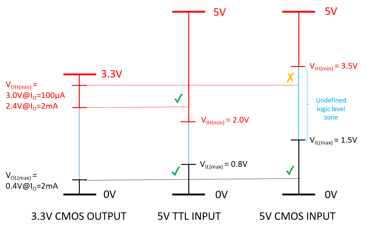
Fig.1 Logic levels of a 3.3-V CMOS output, a 5-V TTL input and a 5-V CMOS input.
The main ways to interface a 3.3V output to a 5V input are:
Direct connection
Using a 74HCTxx gate (or other 5-V TTL-input compatible families)
Using a diode offset
Resistor Offset
BJT/MOSFET inverter
Series MOSFET
Series BJT
Level Translator IC
Optocoupler/Isolator
DIRECT
CONNECTION
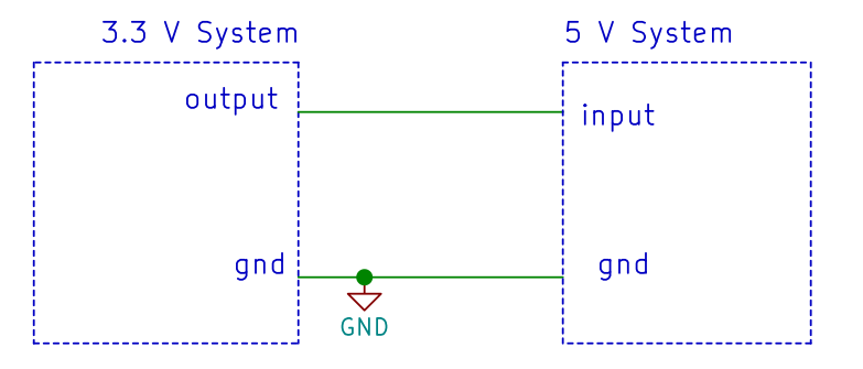
This is the simplest way. This solution “almost always” works, but with some important warnings.
Fig. 2. Direct connection between a 3.3V CMOS and a 5V TTL device is possible.
First, when interfacing with TTL inputs, any “modern” CMOS output
will work, as the high level output voltage of a 3.3V CMOS is close to
3.3V (note! The actual output voltage depends on the output current. For
heavily loaded outputs, the output levels might vary of 0.5V or more!),
still the minimum high-level input voltage for a TTL is 2V. Similarly,
if not too much heavily loaded, the low-level output voltage of a CMOS
is lower than the maximum low-level TTL input voltages.
We wrote “modern” CMOS because older CMOS chips (e.g. CD4xxx series)
have a very high output impedance, therefore they cannot sink/source too
much current (you generally do not want to sink/source more than 0.5
mA). Trying to get too much current will make the output voltage shift
too much. Older TTL chips have an input current, which might exceed 1mA.
Almost all modern CMOS devices (e.g. the GPIOs of MCUs) allows driving a
much higher current without problems.
Second, when interfacing to a 5V CMOS devices, this might work, but not reliably. In fact, the high level input voltage of a 5V CMOS is 3.5V. This is even higher than the maximum output voltage you might expect from a 3.3V system (i.e. 3.3V). Still,
why this generally works ? The answer is due to the actual threshold
logic level, which is 2.5V for a 5V CMOS. Any voltage above 2.5V would
be read as 1, and any voltage below 2.5V would be read as 0.
However, the actual threshold level might shift with temperature and
aging: operating between the two logic levels region is not safe. Any
noise or disturbance might produce a glitch at the output. If your
system must work reliably, then you need other solutions, as shown
below.
Furthermore care should be taken when driving a digital non hysteretic
input close to the logic level threshold, as current consumption would occur.
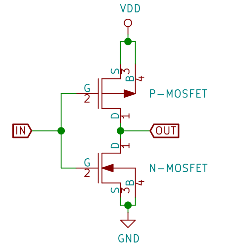
In fact, consider the simple CMOS inverter, shown below: when the input voltage
is close to the VDD/2, both MOSFETs are in the ON state, therefore a direct
path current will flow from VDD to GND.
Fig.3.
The internal circuit of a CMOS inverter. If the voltage at the “IN”
signal is close to VDD/2, then both MOSFET will be in the ON state, and
current will flow between VDD and GND..
Advantages:
No
additional components!
Fast
Disadvantages:
Reduced
noise margins.
Works
reliably only with some logic families.
USING A 74HCTxx GATE (or any other logic family with TTL compatible inputs)
The 74HCTxx family series are CMOS devices with TTL compatible logic
levels (all the other 5V logic families that have TTL compatible input
levels will work too) . In particular, the input high-voltage level is
2V, which is well below the CMOS high output voltage. By inserting any
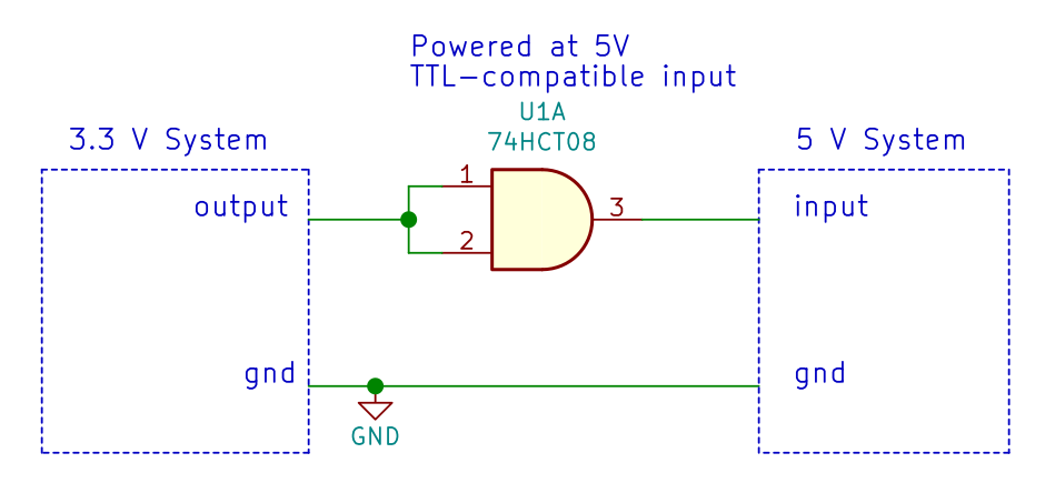
logic gate (see examples below) with TTL-compatible input levels between
your systems, you create a suitable voltage level translator.
Fig. 4. Any non-inverting logic gate with TTL compatible inputs can reliably perform as translator.
Advantages:
Fast
Works
with both CMOS and TTL devices
Need
only one power supply.
Disadvantages:
Requires
an external IC (and possibly its decoupling capacitor)
USING A DIODE OFFSET
With the
direct connection to a 5V CMOS input, we saw that the main issue was the high
level output voltage of the 3.3V output, which is not high enough to be just in
the safe region (3.3V at most, vs 3.5V minimum). Instead, the maximum voltage
of a low level CMOS input is 30% of VDD, i.e 1.5V in a 5V system. Therefore, if
we could add small offset to the CMOS output, that would be great. For this
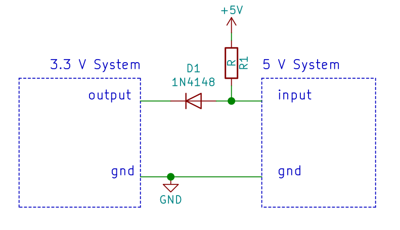
reason, one could simply ad a diode and a pull-up resistor.
However, in
this way, current will flow into the output protection diodes of our 3.3V
system. Such current should be made as small as possible, to avoid damaging the
3.3V system.
Fig.
5. The circuit above introduces a 0.7 to 1V offset (depending on R1
value). However, reverse current will flow into the output even when it
is in the high state. This might cause issues on the 3.3V device.
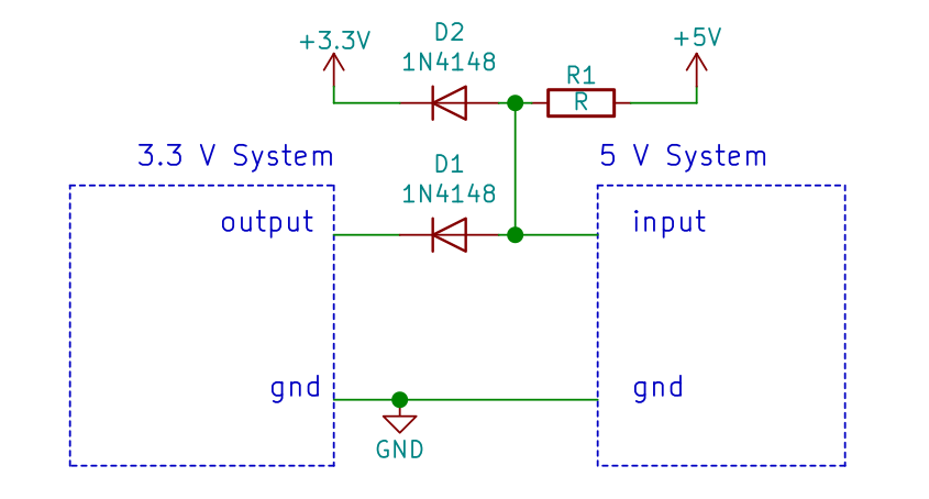
A better
solution is to use an additional diode. Since the new diode is directly connected
to the 3.3V rail (it does not have to pass through our IC), the current will
flow preferably there.
Fig. 6. In this circuit, when the output is high, the current will not flow into the output, but across D2.
Still, both
these solutions has an intrinsic problem: if the 3.3V system is really low
power, then of course it will consume a very low current. If the total current
consumption is lower than the current flowing into the resistor, then
effectively, the 3.3V rail will be powered by the 5V, through the resistor and
diode.
This might
be an issue, as, if no enough current is drawn by the 3.3V system, the 3.3V
voltage might increase up to about 4.3V, which could damage the 3.3V system
itself.
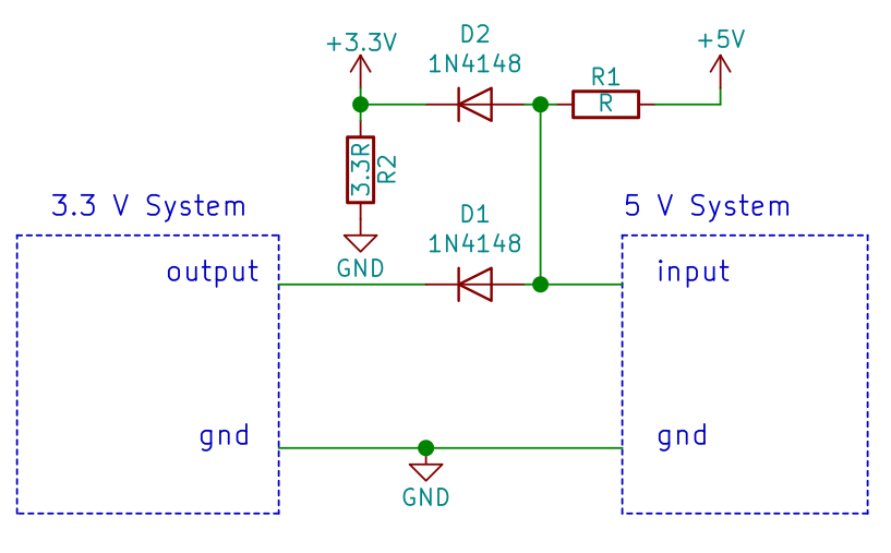
A simple solution is to put a second resistor, which draws at least
the current that would flow into D2 (about 1V/R1. Therefore R2 should be
3.3 times R1 or less).
Fig.
7. Adding R2, with a value at most 3.3 times larger than R1, we are
sure that the current flowing into D2 will be “dissipated”, and will not
increase the 3.3V voltage.
The value
of the pull-up resistor should be calculated so that:
It
is low enough to grant us the desired speed.
It
is much smaller than the input impedance (though in a CMOS device, this is not
much an issue).
It
is large enough, not to overload the CMOS output voltage, especially at low
level. This is especially an issue on those CMOS output with relatively high
output impedance (CD40xx series).
It
is large enough, to avoid too much current flowing into the 3.3V rail.
It
is large enough, to keep current consumption at an acceptable level.
Advantages:
Cheap
Disadvantages:
Much slower than other solutions.
Requires a careful
resistor value selection: to avoid damage, to get a decent speed, and to
keep the high and low voltage within the correct ranges.
Relatively high current consumption.
Requires 2 to 4 additional components.
Poor noise margins.
Requires a low impedance driving output.
Requires a relatively high input impedance
RESISTOR OFFSET
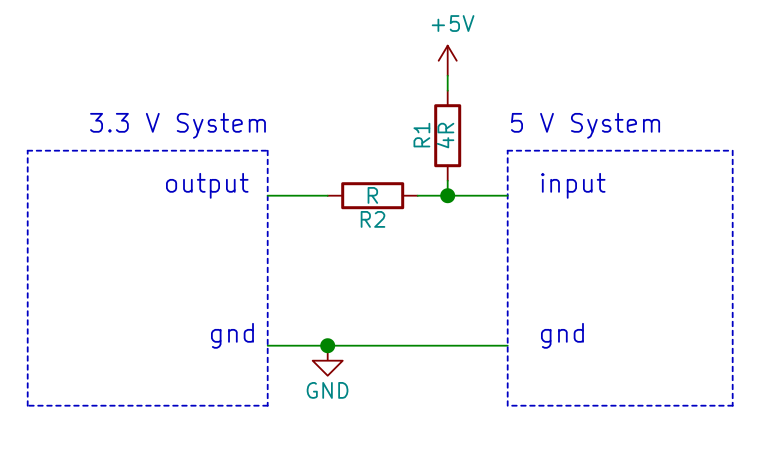
We can
introduce an offset also using a resistor divider too.
This simple
solution is cheaper (but somewhat slower) than the diode-offset, and still has
the problem of current flowing into the output pin.
Fig. 8. A simple resistor divider will allow to add an offset to our 3.3V output.
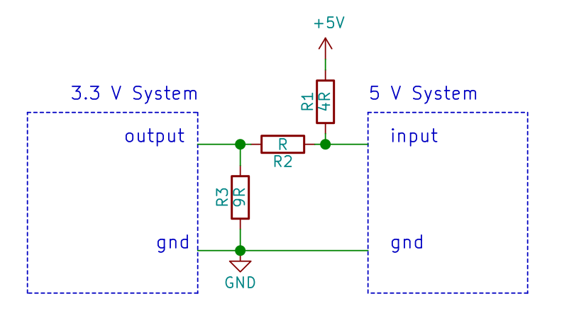
A better solution is to add a dummy load to the output, that will
adsorb the current coming from the 5V through R1 and R2. Another way to
view this, is that, disconnecting the output, with the calculated value,
R1-R2-R3 will form a resistor divider and the voltage across R3 would
be 3.3V at most. The values indicated in the figures are expressed in
terms or a generic “R” value.
Fig.
9. Adding R3 will allow to shunt to ground any current coming from the
5V (instead to 3.3V through the output pin), when the output is at 3.3V.
When the output is 0, the voltage will be 5V * (R2/(R1+R2)), i.e. 1V,
which is below the 1.5V threshold. When the output is 3.3V, the voltage
will be 5V * (R2/(R1+R2)) + 3.3V * (R1/(R1+R2)) = 3.64V. Better
high-level values can be achieved by adjusting the R1/R2 ratio, but you
must take into account that the voltage should be smaller than 1.5V,
when the output is at 0V.
Note: we took 0 and 3.3V as the CMOS output voltages, when the output
is low and high, respectively. While, this time, there is no problem
(unless R3 is too low) about the high level voltage (as it is pulled up
by R1+R2), the low-level voltage will increase according to the current
flowing into the output.
Advantages:
Cheaper
than diode offset.
Disadvantages:
Slower
than the diode offset solution, especially in the high-to-low transition, as
the current flows across R1 and R2, which will have a much higher impedance,
with respect to a diode.
Requires
careful resistor value selection, to avoid damage, to get a decent speed and to
keep the high and low voltage within the correct ranges.
Relatively
high current consumption.
Requires
2 to 3 additional components.
Poor
noise margins.
Requires
a low impedance driving output.
Requires
a relatively high input impedance.
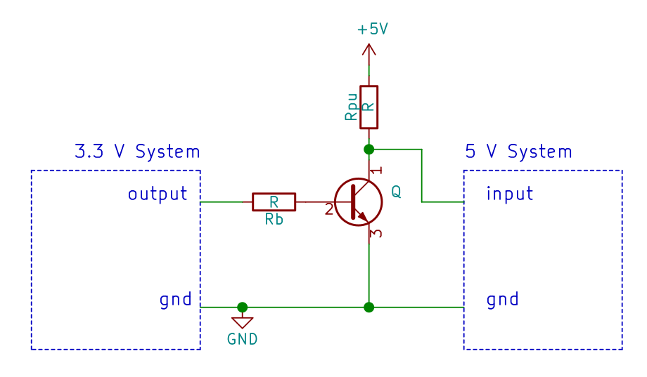
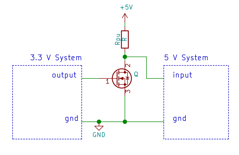
BJT/MOSFET INVERTER
As we did
in the other article, a simple MOSFET/BJT can be used, if an inverted signal
can be accepted or is desired. Otherwise, an additional stage can be used.
Fig. 10. Simple BJT inverters. Cascading two of them will allow to achieve a direct signal, instead of a negated oneFig. 11. MOSFET version of the previous figure. Less components, but more expensive.
Advantages:
Much simpler dimensioning, with respect to the diode offset.
Better noise margin, as both the low and high levels are close to the rails.
Disadvantages:
Requires
2/3 external components.
It
is inverting.
Relatively
slow low-to-high rise time.
The
BJT implementation is actually relatively slower, with respect to MOSFET implementation,
due to the relatively slow BJT turn-off characteristics.
Relatively
high consumption, when the MOSFET/BJT is in the ON state.
Requires
a relatively high input impedance
SERIES MOSFET
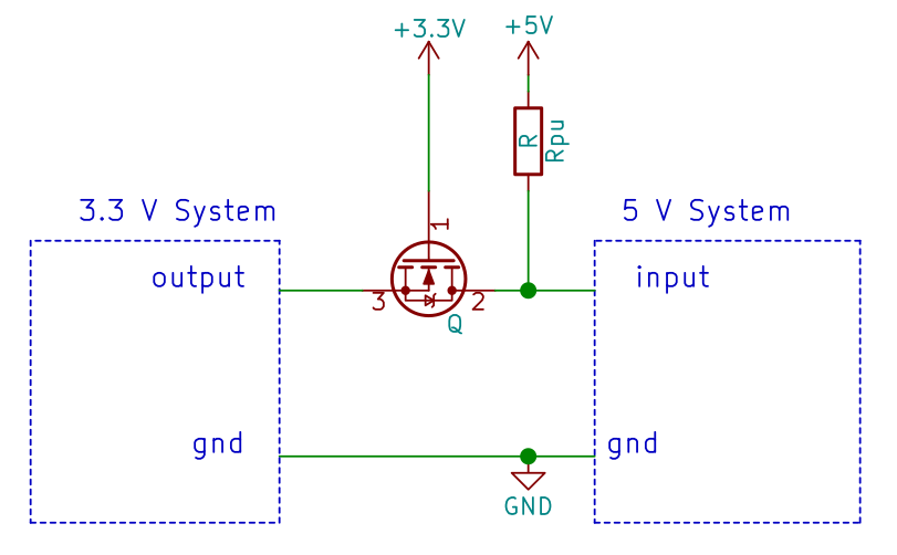
In the
5-to-3.3V article, we showed this little circuit, and we told that it is
bidirectional. Indeed, it can be used for 3-to-5V translation too!
Fig. 12. Single MOSFET level translator.
The working
principle is simple. When the output is at 3.3V, the MOSFET will be in the
OFF-state, as VGS=0V, therefore the output is held at 5V by the pull-up resistor.
If the output is low, then VGS is 3.3V. Assuming a MOSFET with a logic-level
threshold (it should be fully-on when VGS = 2.5V), the MOSFET will turn on,
passing the low-level value to the 5V input.
Advantages:
Bidirectional
Relatively
simple solution.
It
does not invert the input, as the single MOSFET/BJT in common source
configuration.
Disadvantages:
Requires
2 external components
Relatively
slow.
Requires
a low-impedance driving output to avoid overload.
Relatively
high power consumption.
Requires
a relatively high input impedance.
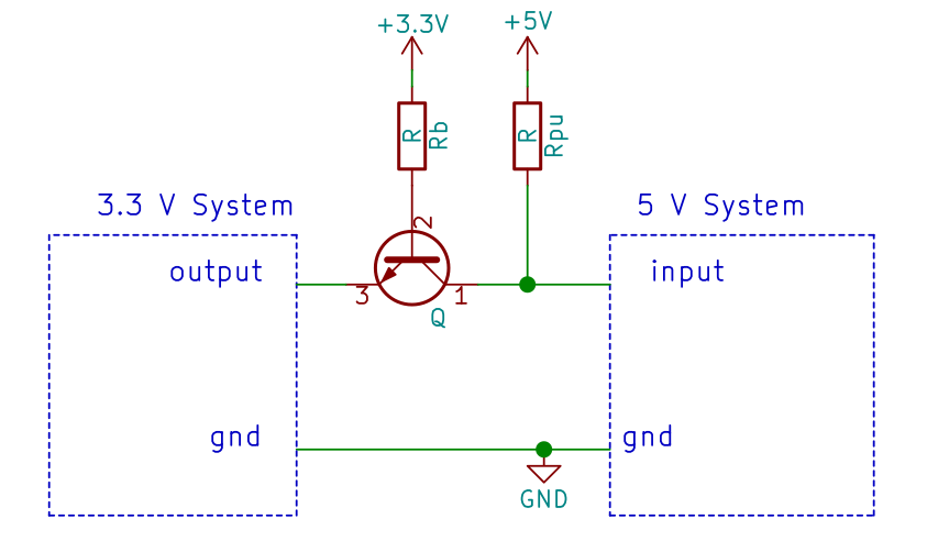
SERIES BJT
This is the
brother of the previous solution, except it uses a BJT. The working principle
is the same (as we also explained in the previous article). It shares the same
benefits of the previous circuit, but it also introduces some additional
drawbacks.
Fig. 13. Single BJT level translator.
Advantages:
Bidirectional
Relatively
simple solution.
It
does not invert the input, as the single MOSFET/BJT in common source
configuration.
Disadvantages:
Requires 3 external components.
Relatively slow.
Requires a low-impedance driving output to avoid overload.
Relatively high power consumption.
Requires a relatively high input impedance.
The BJT saturation collector-to emitter voltage (VCESAT) is added to the low-level output voltage. This is normally not a big deal, though.
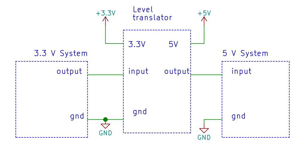
LEVEL TRANSLATOR IC
A dedicated level translator IC, such as 74LVC1T245, will do
everything you need, with better performances with respect to discrete
solutions, but at a much higher price.
There are many variants, such as with more channels (74LVC8T245,
74LVC16T245), or different logic family (74ALVT162245), with different
speeds (and prices).
Use this solution when you require a high performance 3.3V to 5V level translation (typically in high speed buses, clocks, etc.)
Fig.
14. A level translator will generally perform better with respect to
the other solutions, especially in terms of noise margin and speed
(except direct connection).
Advantages:
Fast (even though not as fast as the direct connection, as a small delay is added).
High noise margin.
Disadvantages:
Requires
a level shifter and possibly 2 decoupling capacitors (one per power domain).
Expensive.
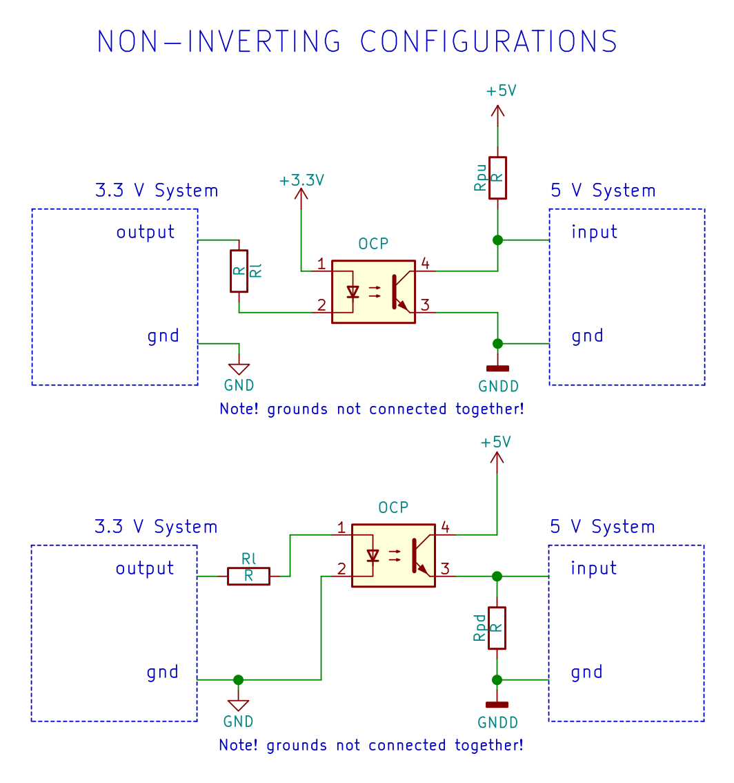
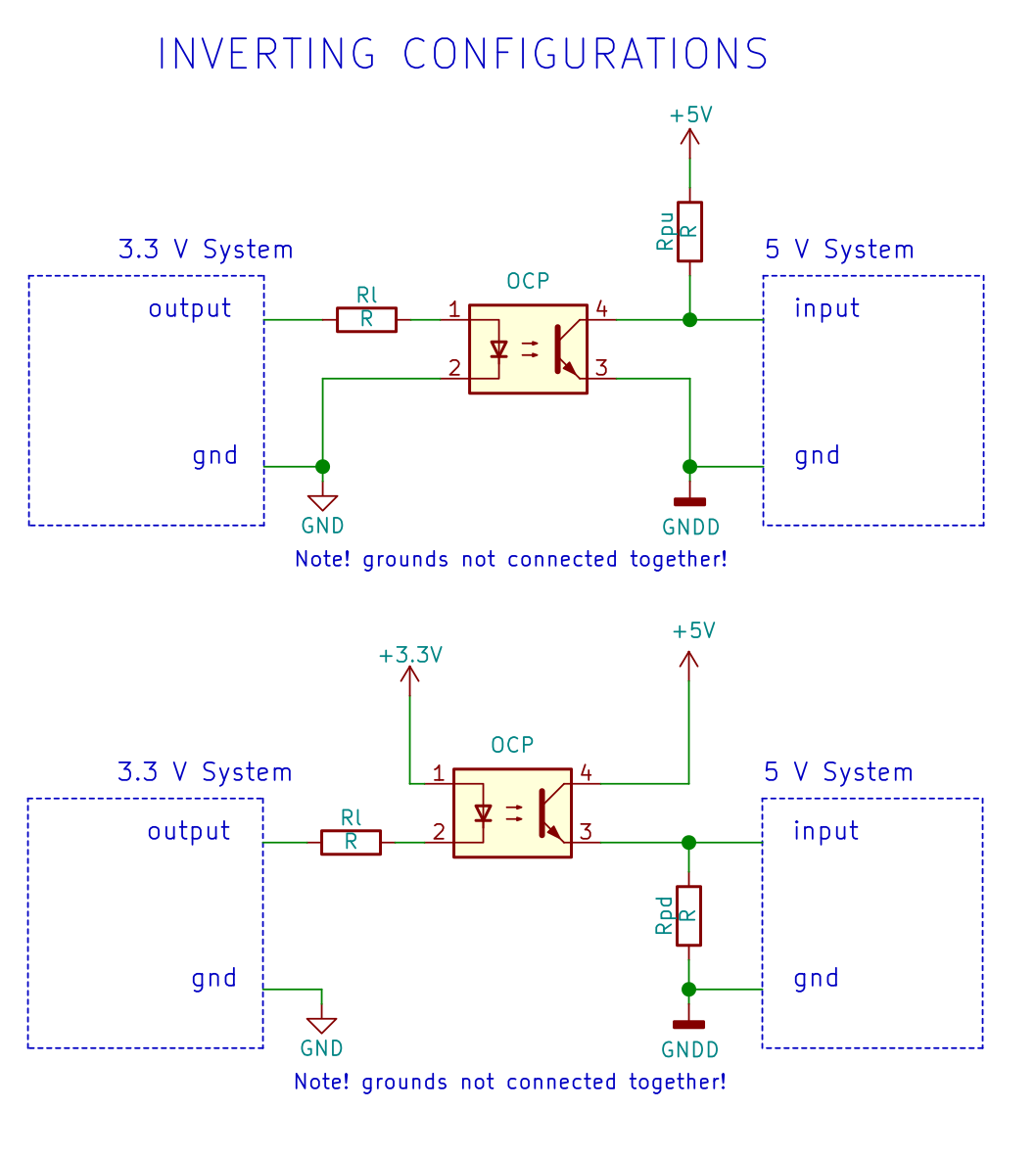
OPCOUPLER/ISOLATOR
As shown in
the previous article, this solution is “any voltage-to any voltage” translator,
therefore it can be used also for the 3.3V to 5V translation. There are 4
configurations, depending on your requirements.
Fig. 15. Non-inverting configurations using optocouplers. Fig. 16. Inverting configurations, using optocouplers.
Beware that
some configurations require a strong low-level output driver (while nothing is
requested in terms of high-level output strength), while the other requires a
strong high-level output driver.
Similarly,
the output will provide a strong pull-up/down path (through the coupler), and a
weaker one (through the pulldown/up resistor, respectively).